4 To 16 Decoder Logic Diagram

Sequential And Combinational Logic Circuits Types Of Logic

Sequential And Combinational Logic Circuits Types Of Logic

Binary Decoder Circuit Diagram With Images Circuit Diagram

Pin On Girls

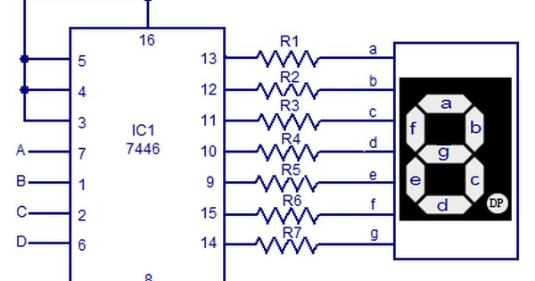
Bcd To 7 Segment Display Decoder Construction Circuit

Ht12d Circuit Diagram Circuit Diagram Circuit

Importance is given to making.
4 to 16 decoder logic diagram. For n inputs a decoder gives 2 n outputs. Pinning information 5 1 pinning fig 4. It is the reverse of the encoder. Vm 1 3 v.
4 to 16 line decoder demultiplexer 5. September 1993 8 philips semiconductors product specification 4 to 16 line decoder demultiplexer with input latches 74hc hct4514 ac waveforms fig 6 waveforms showing the input a n le e to output q n propagation delays and the output transition times. Draw the logic diagram of 2 to 4 line decoder using a nor gates only b nand gates only duration. The input a b c and d can represent any logic function and the output 1 through 16 will then provide the addition or the logic or function of these four inputs.
2 to 4 line decoder with enable input truth table. Let s learn together 971 views. The block diagram for connecting these two 3 8 decoder together is shown below. The block diagram of 4 to 16 decoder using 3 to 8 decoders is shown in the following figure.
Fig 7 waveforms showing the minimum pulse width of the latch enable. Draw the logic diagram of a 2 to 4 line decoder using a nor gates only and b nand gates only. Required number of 3 8 decoder for 4 16 decoder 16 8 2 therefore we require two 3 8 decoder for constructing a 4 16 decoder the arrangement of these two 3 8 decoder will also be similar to the one we did earlier. The complement of input a3 is connected to enable e of lower 3 to 8 decoder in order to get the outputs y 7 to y 0.
There is no electrical or mechanical requirement to solder this pad. Active 3 years 5 months ago. 74154 4 to 16 decoder logic diagram. A decoder is a combinational circuit constructed with logic gates.
A decoder circuit is used to transform a set of digital input signals into an equivalent decimal code of its output. The substrate is attached to this pad using conductive die attach material. Vi gnd to vcc. Include an enable input.
The parallel inputs a 2 a 1 a 0 are applied to each 3 to 8 decoder. Here the outputs y0 to y7 is considered as lower. Ask question asked 5 years 11 months ago. Logic diagram dde 1 this is not a supply pin.
Vi gnd to 3 v. Electrical engineering stack exchange is a question and answer site for electronics and electrical engineering professionals students and enthusiasts. September 1993 7 philips semiconductors product specification 4 to 16 line decoder demultiplexer 74hc hct154 ac waveforms fig 6 waveforms showing the address input a n to output yn propagation delays and the output transition times.

Fpga Bcd To 7 Segment Decoder Schematic Need Help Fitting In

74ls138 Decoder Pinout Electronics Circuit Diy Electronics Circuit

Pin On Electronics

Pin On Ciekawe Schematy

Priority Encoders Encoders And Decoders Simple Explanation
7446 Seven Segment Decoder Driver Circuit Diagram Esquemas

Schematic Transmitter 883x1024 Dc Circuit Electronics Projects

Arduino Dcc Function Decoder Modelisme Ferroviaire Modelisme

Verilog Code For Decoder Coding Projects To Try Projects

4029 Up Down Counter With Images Seven Segment Display

Pin On Elektronika

4 Function Dcc Decoder Wiring With Images Model Railway Track

Microcontroller Pin Definition With Images Microcontrollers
